VHDL Communications for an External 7 Segment Display.
A. Summary
The design needs to be implemented using the Xilinx Vivado CAD software and be designed for and tested on the Nexys4 board. It will also utilize Xilinx’s single port ROM IP-Core. An external piece of hardware that must be used is the Sparkfun 7 segment display. The overall goal of this problem is to produce and display a premade sequence from an IP-Core ROM to onboard and an external display. The external display needs to be able to be controlled using TTL, SPI or I2C meaning all three must be designed and implemented. The sequence that is being displayed should go in the forward direction by default but react to button presses. One button must asynchronously reset the system, another must enable/disable the change of sequence and the other will control the direction the sequence goes. These buttons must be debounced and implemented properly. This system was thoroughly tested and was successfully implemented on the Nexy4 board. It performed to specifications given in the design problem as well cohere to good design practice for maintenance and reusability.
B. Design Problem Statement
Our design is a 7-segment controller that takes three button inputs and a clock as input from the FPGA and outputs the HEX sequence:
'0000, 0A0A, 5050, FE45, AABB, CCDD, FEED, DEAD, BEEF'
on the 7-segment display. This sequence should repeat when it is operational, and should be displayed on the 4 7 segment displays on the right side of the board. The design is implemented using Xilinx's Vivado CAD tool. This sequence is stored in Xilinx's single port ROM/RAM IP-core for this design. This design uses a specific sequence of values, but should be designed generically in a way that would make it easy to display a different signal. The design calls for an “effective clock” of 1 Hz and will control which value will be displayed. This will allow each number in the sequence to be displayed for one second. The design also calls for a reset button that will allow the system to restart at the beginning of the sequence one second after the button is depressed; BTNC on the Nexys4 should perform this function. A reverse button that will toggle the system to output in the reverse order if pressed; BTNL should perform this function. An enabler button that will stop the sequence from changing if it is pressed and will allow it to continue from where it left off if pressed again; BTNR should perform this function. These buttons need to be debounced in order to retain proper functionality. In addition to the 7-segment displays on the board, this design specification also calls for the system to display a 16 bit HEX number on an external display, namely the Sparkfun 7-Segment Serial Display. This is to be designed using a TTL Serial Communication controller, an SPI Serial Peripheral controller as well as an I2C controller utilizing and I2C master blackbox to display the signal on an external serial 7-segment display. These two design methods are to be separate entities and are self-contained designs. Finally, the design, as well as the individual modules, was to be tested and analyzed using a Testbench in Xilinx’s simulation tool in combination with the LeCroy Logic Analyzer.
C. Problem Decomposition
 Figure 1: Top level block diagram
 Figure 2: RTL Block Diagram
In order to keep the design modularized and easy to modify/reuse, the top level design needs to be broken up into individual blocks. Starting with the inputs to the overall system, there should be either one block or three separate blocks to handle the button inputs. The code provided by Digilent allows the buttons to be handled in three separate and easy to use black boxes that allow for toggling as well as simple debouncing.
Figure 2: RTL Block Diagram
In order to keep the design modularized and easy to modify/reuse, the top level design needs to be broken up into individual blocks. Starting with the inputs to the overall system, there should be either one block or three separate blocks to handle the button inputs. The code provided by Digilent allows the buttons to be handled in three separate and easy to use black boxes that allow for toggling as well as simple debouncing.
Logically, since the buttons are used to control a sequence the next block should be a sequence controller that handles the buttons as well as determining what the current sequence to display should be. That means that the sequence controlling block would need to have the three debounced buttons as inputs as well as the clock from the Nexys4 board. The sequence controller would need to control the ROM to output the current data to be used by the individual displaying blocks. It would need to do this by changing the address to the ROM and obtain a new 16 bit output every 1 second, or at a 1 Hz rate. At the same time it would need to properly react to button presses; changing back to the beginning for reset, switching direction for reverse, and stopping the switch for enable.
Based on the design for the sequence controller as well as using the modular design concept, the output portions of the design should be kept as separate block entities for each form of output. First, the onboard display should have its own block as it does not relate to the other forms of output. This block should only need to take in the board clock as well as the current data from the sequence controller. From this, the board display block should be able to properly display the hex sequence across the right side 7 segment display. Since these are not set altogether but rather individually, this means that the block will have to be continuously trying to refresh the 7 segments at such a rate that it would appear to a person that all of them change and are lit at the same time. Also, the onboard 7 segment displays do not have a separate microcontroller for a hex-to-7-segment decoder the board display block should also convert the hex into the correct setting for the active-low 7 segments. That means the board display block will have two vector outputs, the anodes for the 7 segment and the cathodes.
The next output module would be the serial TTL communication for the external display. As with the board display block this would only need the data and board clock as inputs to the module. The block itself would need to break up the data into individual bytes and send them through the TTL protocol at a rate of 9600 baud. With generics, this would be easily adjustable for any external display. That means that this block would only need to have a single output in the GPIO.
Another output block, for the SPI communication, would follow suit in terms of inputs needing only the board clock as well as the current data from the ROM. Since SPI is more robust than TTL, the block must do more than simply send bytes, it must be a state machine that controls three different lines of the GPIO of the Nexys4. Apart from breaking up the 16 bit data into bytes, the block must send them out according to the predefined SPI communications. This requires three lines, the serial clock (SCK), the slave select (SS), and the master-out slave-in (MOSI).
Finally, the I2C protocol must be adhered to in the i2c controlling block. Due to the modular design of the system, this should also only require the board clock with the data in order to be functional. In this design there is black box i2c master provided so this i2c controlling block is to be designed around this. Internally then, the i2c controller would need to contain the i2c master and use it to properly send the data. In an overview sense, this block needs to run the i2c master in a manner that would produce desirable outputs. This requires a state machine to initialize internal components as well as write and stop the data flow. Because this still follows I2C protocol there would be two ‘outputs’ which are actually input-outputs. They are SDA and SCL; technically input-output lines however for the purpose of the current design the input portion is only used for acknowledgements rather than transferring data.
D. Detailed Design and Module Level Testing
Overall, because the design was designed with a modular basis, the individual blocks can be analyzed for their function and then the interaction between them can be seen and understood. This also allows for blocks to be reused in future designs. The RTL diagram provided by the Vivado CAD tool is shown in the appendices as well as the source code.
####Button Debouncing: This portion of code does not have much complexity and is easy to recreate. Although this code is provided by Digilent, the design is very straightforward making it easy to understand and utilize. In simple terms the code detects a button press then begins to count up to a pre-specified number. Upon reaching the maximum value, the code checks if the button is still at a logic ‘1’ value. If it is, then the debounce signal goes high. The counter then begins again; once the button signal goes low. When reaching the maximum value, if the button signal is still low then the debounce signal follows and falls low. It is able to check for these by using a simple “xor” of the signals for the debounced button and the hardware. The toggle is simple as long as the debounce code is written and functioning. A register of the debounce signal is used to check and see if there was a change in value. If the signal goes from a low to a high, another signal, for the button pulse, goes high for one clock cycle which changes the value of the toggle to the opposite of the previous value.
####Sequence Controller: The generic job of this component is to generate numerical addresses for a ROM at the speed of 1Hz. The only part that adds complexity to this portion of code is the handling of the buttons. This code must utilize a clock enabler which activates every 1 second, a very simple piece of code. Using this, the sequence controller will increment the address for the ROM every second given that it is not in reset, not disabled and not counting backwards. The pseudo-code is shown below:
If in reset then
	Reinitialize sequence;
Else
	If still enabled
		Count up or down;
	End if;
End if;
This pseudo-code, when implemented properly, will perform the main function of the sequence controller. Of course, clock and clock enabler checks would still need to be performed in the inner statements for synchronousness but this would allow the reset and the enable to be asynchronous which is what is needed for this design. Also within the inner statement, the handling of minimum and maximum counts would have to be addressed depending on the number of sequences being used.
####ROM: This part of the design is created using Xilinx’s ROM/RAM IP-Core for Vivado and so there is no actual source code to write, this is another one of the black box situations. The instantiation is provided by Xilinx in order to use the ROM. The sequences are loaded in by creating an initialization file for the ROM which already contains the sequences. The ROM outputs the sequence that corresponds to the address that is generated by the aforementioned sequence controller.
####Board Display: The board display block uses a clock enabler that runs at the refresh rate desired by the user, this is a generic value. In order to correctly make a board display for this design, there needs to be a counter, sensitive to the clock enabler, which has a maximum of four values because we are using four seven segment controllers. This can also be done as a state machine but for simplicity a counter is used. The basic idea of the counter is to select which seven segment and its corresponding data. For instance, at the first value of the counter the module should select the anode for the furthest right display and the least significant hex of the data sequence. This is illustrated below using the sequence of “BEEF.”

Figure 3: The main function of the board display module.
In the above figure, the red for the text represents which part of the text should be selected and the red of the 7 segment represents which segment or anode to choose. Because only one turns on at a time, this must be done with a high refresh rate in order to fool a human eye into thinking they are all displayed at once. This generic value is set at 1KHz. Lastly, when displaying the sequence onto the 7 segments, there is no native way to translate the hex into an active-low logic vector which represents which LEDs to turn on. This deficiency is resolved with a simple case statement that can work for any given hex and active-low display.
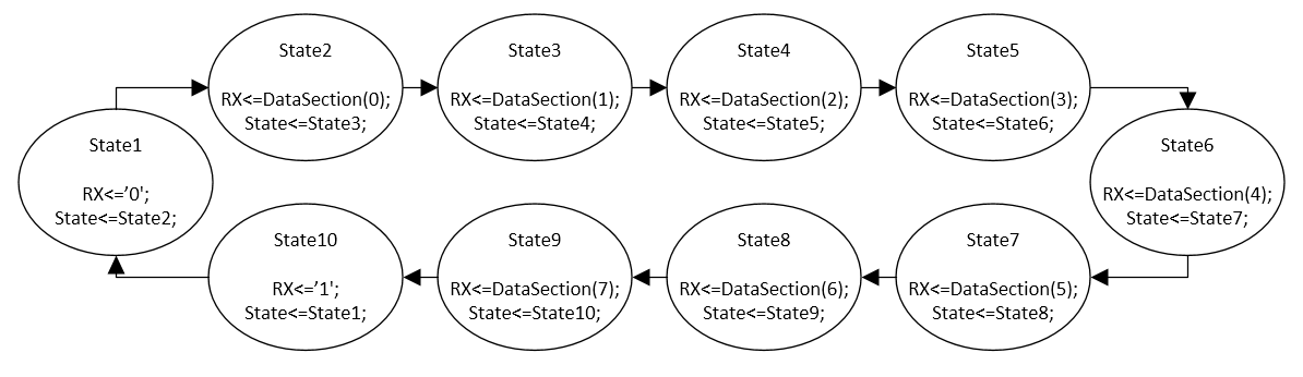
####TTL Communication: In this design, with this external display, the default Baud rate is 9600 which insists upon a clock enabler at that frequency. This baud rate determines the rate of change of a simple 10 stage state machine. In this state machine, the first and last state are used as start and stop bits for communication which the intermediate 8 states are bits determined by the section of data being sent to the external display. An example of the state machine is shown below.

Figure 4: Example state machine for TTL Communications.
In this example there would need to be another signal called “DataSection” that changes on the tenth state either with an internal or external counter. This would allow for initial commands to be sent to the display for setup as well as easily splitting up the data to send out in bytes when new data comes in using case statements.
####SPI Communication: SPI has a much different behavior than TTL mainly because it uses more than one line for sending data. SPI needs 3 lines: Serial clock (SCK), Slave select (SS) and Master-out Slave-in (MOSI). Each slave that is used generally will prefer to run at different speeds but allows a range of speeds sent down the SCK. In this instance this is set, in the generics, to be 250KHz. Using a clock enabler, the system runs at 250KHz with 19 total states. The large number of states is used to artificially create the SCK. A normal clock can be used with some extra logic but for design simplicity the multiple states allows for a gap in the clock to disable the SS. When the SS is inactive, the MOSI is required to be in high impedance mode; otherwise the MOSI is sending the data to the slave reading on the rising edge of SCK (when CPOL=0). This is more easily shown through the waveforms below.

Figure 5: Example SPI waveform.1
Shown by the red lines on the waveform, the data is read in for CPOL=0 on the rising edge of the SCK. Since the SS is an active low line, it stays low for majority of the waveform, only deactivating during the break in SCK. The “cycles” on the waveform represent new pieces of the data to be sent, meaning that what is shown above is only for a single byte. At the end of the cycles there is a gap between the “8” and the high impedance, this just means that it does not matter what the line is, it will have no effect on the system. The states for this module of the design can be shown in the waveform above rather than in an overly large state machine diagram. The states can be easily seen with the first one holding SS at a high. The next 17 states are used to vary the clock at the red and blue lines as well as the data at the blue lines. That means that any given bit will stay for two states starting with the most significant bit first. That 19th and final state comes from SS going back up to a high. Similar to TTL, a case statement with a counter controls what data piece is currently being sent to the external display. Again, this allows for initial commands as well as easily breaking up the 16 bit incoming data.
####I2C Protocol: The I2C component of this design is more complex than the others, not only because I2C is a robust protocol but because a black box I2C master was used to do the design. First in order to design either piece, the I2C protocol should be understood.

Figure 6: Start and stop conditions for the I2C Protocol.2
Depicted above is the required start and stop conditions for transmitting anything through the protocol. The first, of two lines, must fall to a low while the second line stays high. That part of the protocol is fairly simple as well as transmitting data across the line. The bits are simply sent out on the SDA line while SCL pulses when a bit needs to be sent. The unique part to I2C is that several slaves are usually connected to the same lines and in order to interact with one of the slaves, the master sends out the address of the slave it wants to interact with as well as a single bit stating whether the master wants to read or write. Upon doing so, the slave with the corresponding address should pull down the SDA line. If the line is not pulled down by the slave on the ACK clock cycle then the system receives a NACK error, or a “no acknowledgement” error.

Figure 7: Generic example for using I2C.
Shown in the waveforms above, the NACK error can occur on the 9th pulse of SCL. After the acknowledgement is received by the master, it then can send out or read in the data it needs to. After data is sent or read, acknowledgements occur again. Multiple bytes can be sent out before needing to stop and resend the address, however has been found that the maximum number is about 255 bytes.
Since the I2C master was just a black box and not to be designed it’s only necessary to be able to use it rather than make it. However, since the I2C protocol is understood its general design can be easily reproduced by using the example state machine diagram provided by the maker of the I2C master. The general premise of the master is to send out the start/stop bits as well as the data at the correct speed and intervals. During this task it needs to alert the user or controller of it that the system is currently at work as well as if there is any error communicating with slaves. After it is done working it should tell its controller that it is definitely done with the task it was given. This can then give the user the option to either stop the system or perform more tasks. The state machine diagram that shows this in more detail is shown below.

Figure 8: State machine diagram for the I2C master.3
The diagram shows, in more detail, the previous explanation of its operations. The master can detect both acknowledgements as well as read/write data with the option to stop the system when it is needed by the controller.
The I2C controller should be designed in a fashion as to controller the I2C master. This includes setting up the correct address for the slave being controlled in combination with the data. For this specific design, the controller does not have to control data being read in because data is being written to an external 7 segment display. With an I2C master being used in the design, the controller can be less complex; using only three states. The controller needs to initialize the master in order to use it so that leads to an initial or start state which waits for resetting and initializing by having a maximum counter and counting down to 0, as well as providing the address and desired action of writing. Then the state for writing because it needs to change the data in nearly the same manner as the other output blocks of the design, where it cycles through a set of commands then chunks of the sequence from the ROM. The final state should stop or disable the master once the data is done being sent. This final state should only go back to the beginning on a change in the data. This is illustrated in the state diagram provided.

Figure 9: State machine of the I2C controller.
The pseudo-code for this is shown below.
When Start state:
	If counter /= 0
		Activate master reset
		Disable master
		NextState<=Start state;
		Count down
	Else
		Disable master reset
		Re-enable master
		Set the address
		Set the read/write
		NextState<=Write state;
	End if;

When Write state:
	storedData<=Data being written;
	previousBusy<=Busy from master;

	If Busy goes to 0 then
		If not at the last byte then
			Choose a new byte to send
			NextState<=Write state;
		Else
			Reset byte choice
			State<=Stop state;
		End if;
	End if;

When Stop state:
	Disable Master

	if storedData /= Data From Rom then
		NextState<=Start state;
	else
		NextState<=Stop state;
	end if;
This design resets the byte choice back to the command to reset the cursor back to the beginning in order to ensure the data writes on the correct 7 segments. In this pseudo-code it’s shown that there is a need to control the master directly. Since the controller controls the master, a simple hierarchy is made with the controller containing an instantiation of the master which allows for the easy mapping and controlling as demonstrated in the pseudo-code. This also avoids the hassle of mapping everything across the top level file.
####Hardware Setup: Shown below is the external hardware used in this design. This is the 7 segment display from Sparkfun which supports several communication protocols, including those used in this design.

Figure 10: The generic setup of the external 7 segment display.
This 7 segment is designed to be used with Arduino tools but can be used with any device that uses a recognized protocol. Since it is usually used with Arduino however, it has two sets of power and ground, shown on the top row as “VCC” and “GND” as well as on the bottom row except the ones on the bottom row are meant to be used with Arduino programming.4 Shown below is the hookups for the protocols used in this design, again these can be used with the VCC and GND of the bottom row.


Figure 11: TTL, SPI and I2C setups shown respectively.
E. Alternative Designs
####Top Level Alternate: This design uses modular design and breaks up tasks into logical blocks with some hierarchy. In this design, the individual output blocks all had the need for the data from the ROM. This led to the decision that the sequence should be handled outside of the output blocks. This makes error checking much easier as there is only one block that works with the sequence as well as the buttons. Also, the design is better for reuse because each output block can be used for multiple sequence sets whereas having the sequence controlling in the same blocks would not allow that. There is a minimal hierarchy in the I2C output block because the I2C controller contains the I2C master so there is no issue with transferring signals in the top level.
####TTL Alternate: The TTL design was done with states. This makes the design very simple and straightforward meaning it is a synchronous system with a single counter to go through the bytes of the data. Another way to do this communication is to create a second counter which is dependent on the first counter to count through the individual bits of the byte given by the first counter. While this is not too much different, the design is not as nice as a rigid state machine that has no counting errors.
####SPI Alternate: This SPI communication used a lot of states which is usually not good design. However, this makes the system completely synchronous and avoids issues from asynchronous logic such as trying to get the SCK to not pulse when the SS is high. This can be done in multiple other ways such as asynchronous logic that says the SCK only pulses when “NOT SS” but timing can be an issue with this method. Another method that has issues with timing is a clock disabler. This would count the number of cycles the SCK and pulse when the SS goes high so the SCK would be synchronous to the rising edge of the clock as long as the clock disabler was low. The states also follow human logic because the waveform can easily be broken up into the states, allowing flexibility in changing the design for re-use.
####I2C Alternate: One of the alternates for the I2C protocol for this design would be to design a new I2C master rather than use a black box. A less obvious alternate would be to constantly resend the same data. This can be done by writing the data then going into the stop state and disabling the master. But, rather than waiting for a change in the data from the ROM, the stop state could count down similarly to the initial state and then reset to the beginning; sending the same data again. Although this would be functional, it would lead to flickering on the external display. Lastly, unlike this design, the byte choice could be reset back to the beginning of the data from the ROM rather than the cursor command. While, again, this would be functional this would lead to error if there is an issue with hardware such as a momentary lapse in amperage or voltage. In this case the sequence would appear to start showing up in the wrong order due to the cursor pointing in the wrong location. Having the cursor command every times helps to avoid that.
F. Sources & References
- Image from: http://en.wikipedia.org/wiki/Serial_Peripheral_Interface_Bus
- Image & Info from: http://www.i2c-bus.org/fileadmin/ftp/i2c_bus_specification_1995.pdf
- Code and diagram: Scott Larson, EEWiki, https://eewiki.net/pages/viewpage.action?pageId=10125324
- Info from: https://learn.sparkfun.com/tutorials/using-the-serial-7-segment-display/